
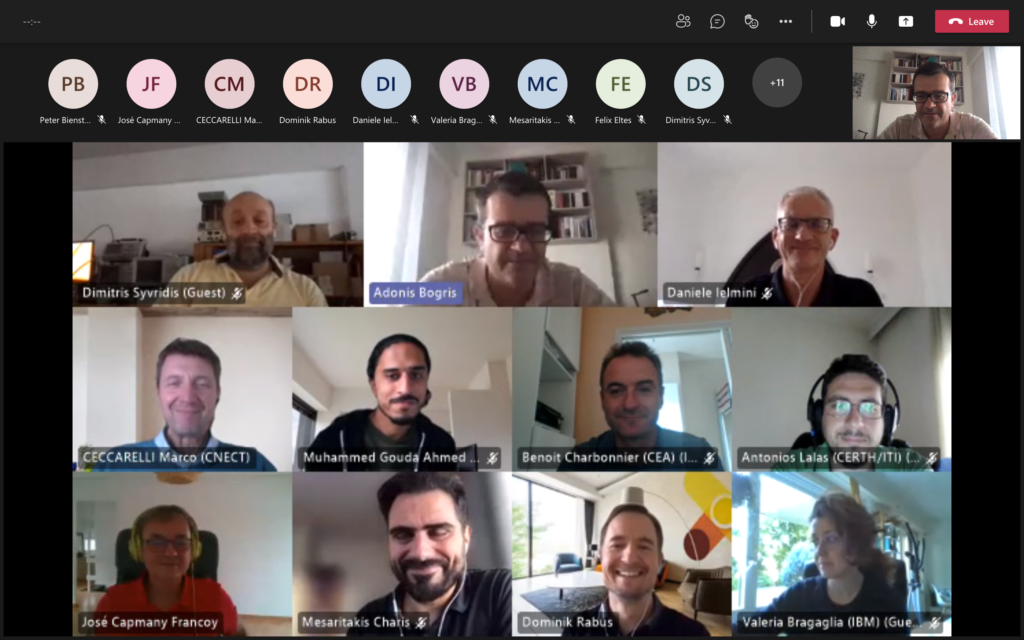
NEoteRIC Midterm review was remotely held last Friday 1st of October with the participation of the partners of the consortium and the Project Officer Dr. Marco Cecarelli, who was for the best assisted by Prof. Daniele Ielmini from Politecnico di Milano and Dr. Dominik Rabus.
The review covered the project activities carried out so far and examined the degree to which the work plan has been carried out, the completion of deliverables, the current relevance of project objectives in providing potential scientific and industrial break through, and how resources were planned and used in relation to the achieved progress. We also seized the opportunity to explain the management procedures and methods of the project and the beneficiaries’ contributions and their integration. Finally, our plan for disseminating and exploiting results was discussed in depth with the reviewers, who could assess the expected scientific, technological, economic, competitive and social impact of the project.
We much appreciated the support and congratulations from Prof. Cecarelli, Prof. Ielmini and Dr. Rabus, as well as their feedback and substantive improvement suggestions, always from a constructive approach.
We are also delighted to announce that a 1 year extension has recently been approved by the European Commission, what will allow us to complete the scientific goals despite of photonic integrated circuits fabrication delay due to COVID related causes. Foundry lockdown, partial service caused by COVID mitigation actions and the large wafer backlog at reopening, forced to schedule a new roadmap, which is based on the following assumptions in order to ensure that the goals of the project will be met in time:
a. Second generation of FPPA circuits will be exclusively based on thermo-optic (T.O.) phase shifters. It will increase the density and the number of nodes comparing to the first generation so that it can be used for real applications. No BTO phase shifters will be included in this device.
b. A separate packaged low-scale BTO reconfigurable chip device will be fabricated to be used as proof of concept of BTO photonic programmable chips. It will mainly demonstrate the low consumption of this technology and will be designed so that it will require the same packaging process as the first generation of T.O. chips to cut down costs.